Load boards
EDA Import & Export
Open the load board your layout tool drew — Allegro first, then KiCad, EAGLE and the rest — natively, with no Cadence licence needed on your side. View the copper, check the board against the test program’s pins and channel plan, and hand the plan back to the layout engineer as a first draft in the tool’s own inputs. ATE·IQ reads, views and verifies boards; the layout stays with the tool that drew it.
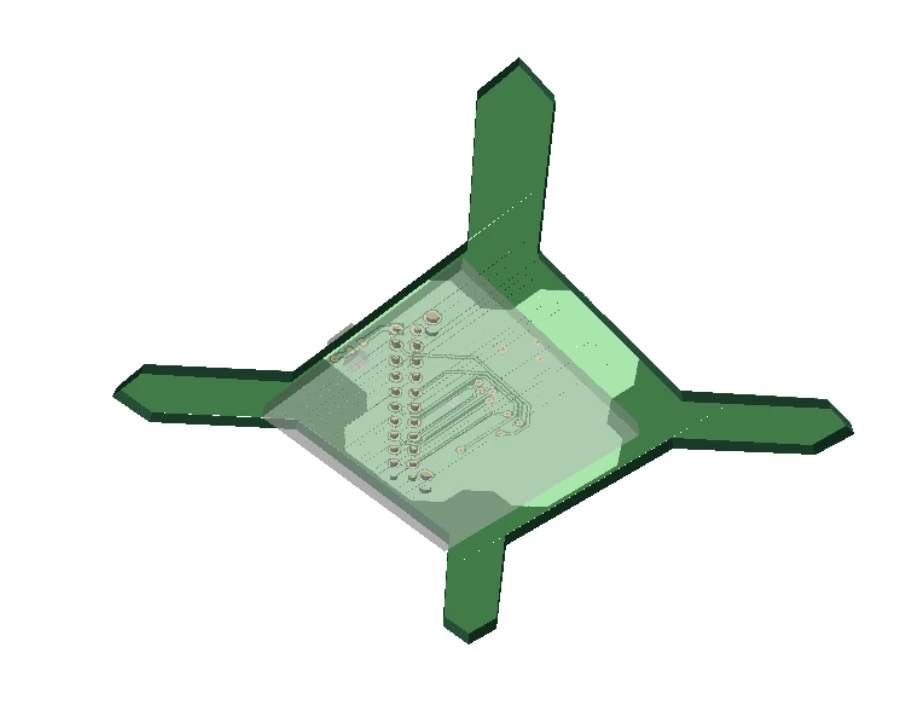
Native readers for the exports your layout tool writes
Many DIBs are drawn in Allegro, and the test engineer rarely has an Allegro seat. ATE·IQ’s own parsers read what the layout tool exports, so a board arrives with no CAD installation beside ATE·IQ. Pick the files from the Import menu, or link the repository they live in.
| Source | What it carries | What ATE·IQ builds from it |
|---|---|---|
Allegro Fabmasterextracta ASCII |
The routed board as Allegro wrote it: pads, plated holes, vias, every etch line and arc, the outline, and copper pours drawn as cut with the voids Allegro left around other nets. | A layout with real copper in the schematic, layout and 3D views, measured by the geometric DRC. Coordinates stay exactly as Allegro exported them. |
Allegro netlistpstchip · pstxnet · pstxprt |
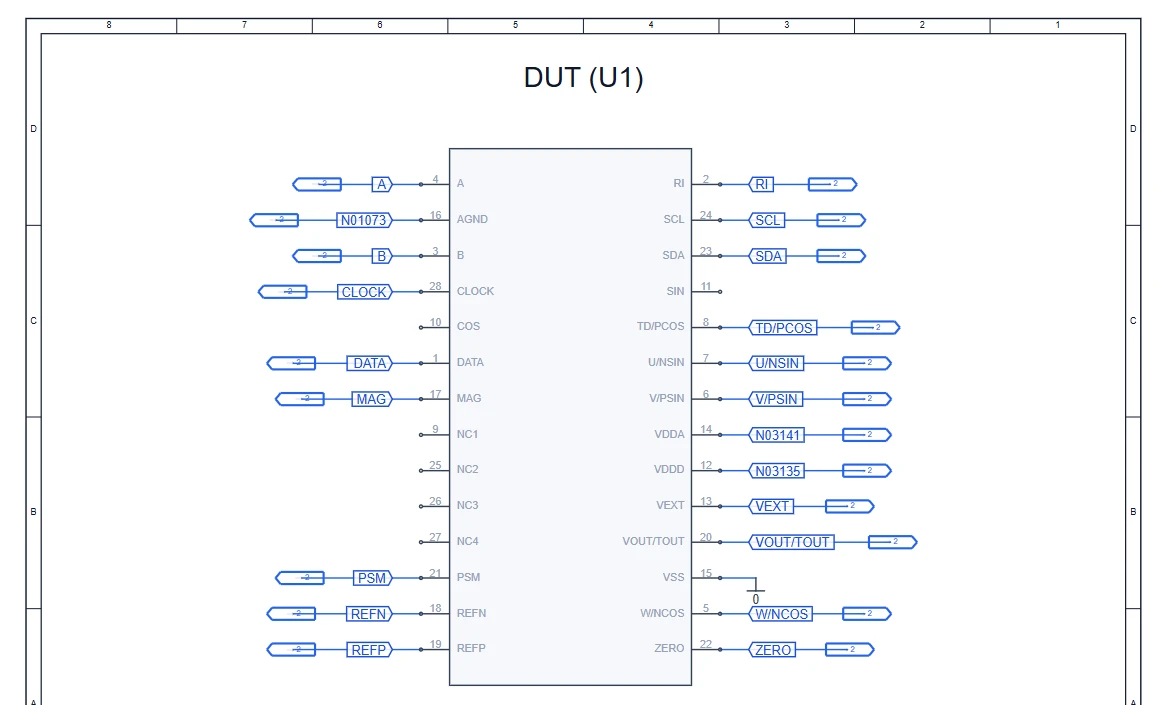
Components, pins and nets as the PCB Editor packaged them. No copper. | A netlist design with a synthesized multi-sheet schematic, enough for the pin match and board↔program sync. Pick the three files together; they are recognised by content, not by name. |
| IPC-2581 | A full board description — components, nets, layers, copper — from Allegro or any tool that writes it. | A layout with real copper. An Allegro export whose films were folded into copper is rebuilt on import (§03). |
ODB++ .tgz |
The layer matrix, the netlist data and every layer’s features. | A layout with real copper, rigid-flex boards included. |
| Specctra DSN | The board in its KiCad, Allegro or EAGLE dialect. | A board with its copper, which round-trips back through an SES session file onto the same design. |
| KiCad | Native schematics and boards from a synced repository. | The schematic as drawn and the board with its copper. |
| PDF schematics | A multi-page drawing, for boards where the drawing is all you have. | A netlist built from the drawing. |
Link a project’s repositories and they are scanned for every format above except PDF, so a board arrives with the program it belongs to. PDF schematics and SES session files are imported by hand.
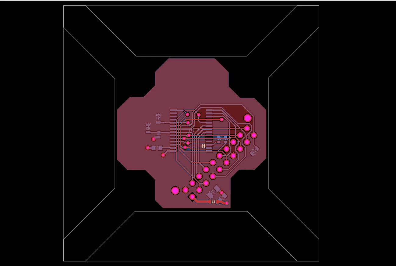
One command on the layout seat
The layout engineer should not have to guess what to send. ATE·IQ provides an export kit for Allegro and OrCAD X PCB Editor: one command on the seat writes everything ATE·IQ reads from the board.
| The kit writes | What it is | In ATE·IQ |
|---|---|---|
| The Fabmaster export | Every component, pin, net, pad, hole, via, trace, arc, pour and the outline. It depends on no film setting, so it is the file to send first. | Import ▾ Allegro Fabmaster |
| IPC-2581 | The board exported with every artwork film mapped to a layer by name. | Import ▾ IPC-2581 |
| The film mapping | The name-to-layer mapping that export used, printed on the seat and saved beside it. Correct a film with an unusual name and run the kit again. | Reviewed on the seat |
| The tool logs | What each export step reported. | Kept for troubleshooting |
The kit drives the seat’s own export tools and uploads nothing: the files land beside the board for you to send, and ATE·IQ parses them on your own machine.
Clean copper from a mixed IPC-2581 export
Allegro’s IPC-2581 exporter folds every artwork film it cannot map by name into the last copper layer, so fabrication and assembly drawings arrive as copper, along with extra copies of the pads. ATE·IQ recognises a folded layer and rebuilds the real one.
The rebuild stands on the file’s own padstack definitions, the side each part is mounted on, and physics. Identical copies collapse to one. A surface-mount pad with no hole cannot sit on the far side of its part. A copy on a pad’s spot with a different shape from the layer’s regular pad is a mask or paste opening. A layer that repeats another layer’s traces verbatim is carrying that layer’s film. A part’s outline that would short two of its own nets is its package drawing. The import notes list what was set aside, why, and the export setting that avoids it. A clean export from the kit in §02 is still the better evidence; the rebuild is there for the file you were sent.
Every import says what it read
Each imported design carries its provenance — which format, which path — and a note, printed on its analysis page, that says what the parser read and what it could not. The checks read it too: a netlist-only import is never asked copper questions, and a layout import is never presented as if it carried stuffing.
“Cadence Allegro Fabmaster (extracta) LAYOUT import — the routed board as Allegro wrote it: components, pins, nets, pads, plated holes, vias, traces and the outline. Copper pours are drawn as cut, with the voids Allegro left around other nets. Stuffing is NOT visible — every placed symbol is listed, fitted or not; confirm against the BOM. Schematic-semantics cards are derived from the layout's nets.”
A check whose input is missing says awaiting data and names the step that unlocks it, instead of rendering an empty chart as if it were a clean one.
From copper to program and data
Once a board is in, check it against the program that will run on it. The geometric DRC measures trace width, clearance and annular ring on the real copper; the 166-rule DIB check runs over the channel plan, the tester configuration and the board; pin match reconciles the board’s nets against the Pin Map sheet; board↔program sync checks every program pin against the bound board; and the traceability dashboard carries the chain requirement → test → net → copper → lot, so a DUT pin points at its program test and its production data. Ask the IG-XL agent about a saved board and it validates and analyses the design in the conversation: its components, its nets, its power rails.

That is the point of reading the board natively: when the loop closes, it closes on the board as its layout tool wrote it, not on a re-drawing of it.
And back out
Integration runs in both directions. The program’s channel contract — the saved channel plan — goes back out to Allegro as the tool’s own inputs: a first-draft netlist for Import Logic and a placement seed for Import Placement, with a disclosed tester-interface placeholder carrying each net’s planned tester channel. The layout engineer starts from the board the program needs, draws the copper in the tool that owns it, and the routed board comes back in through the readers above.
A design also leaves in the formats the fab and other tools take: Gerber and drill files, a one-zip fab package, a BOM and pick-and-place, a KiCad project, Specctra DSN, IPC-2581 and a schematic to print or save as PDF. Fabrication outputs are refused, with the reason stated, for a design that carries no board geometry. The full set is on PCB layout.
.brd files are not read, and OrCAD Capture .DSN schematics are
rejected with a clear message. No customer’s own export has been read yet; where yours
differs, rows the importer does not recognise are skipped rather than guessed at. The
export kit needs a PCB Editor seat on the layout side. The chain from copper to lot has
not yet been shown on a vendor board, and on the demonstration project the copper hop is
not shown: no routed vendor board is bound to it yet, and the dashboard says so rather
than drawing one. The first draft is written by a command-line export, not a button in
the app, and this site shows no draft taken through an Allegro seat. IPC-2581
export carries connectivity only, and passing the fabrication gate means the geometry
exists, not that the board is ready to build.