Design
Schematic Design
The schematic is the logical board — components, nets, and the ATE conventions that make a DIB drawing readable. This is where ATE·IQ authors: schematics are generated from a prompt and the spec, imported from PDF or KiCad, and edited live — and the drawing you review can never drift from the design it describes.
Schematic and layout are different things
ATE·IQ keeps the two concerns separate because they have different owners. The schematic — this page — is the logical design ATE·IQ generates, draws and edits. The layout — the physical copper: pads, traces, pours, drills — usually comes from your CAD flow and is imported verbatim, then checked and exported. That side is covered in PCB Layout.
Both live in one design, stored in an open, MIT-licensed format — so there is no second representation to fall out of sync. A design can hold schematic elements alone (a drawing you generated this morning), or schematic plus copper (a vendor board you imported). Every view shows the same design, and every design records its provenance.
The ATE schematic engine
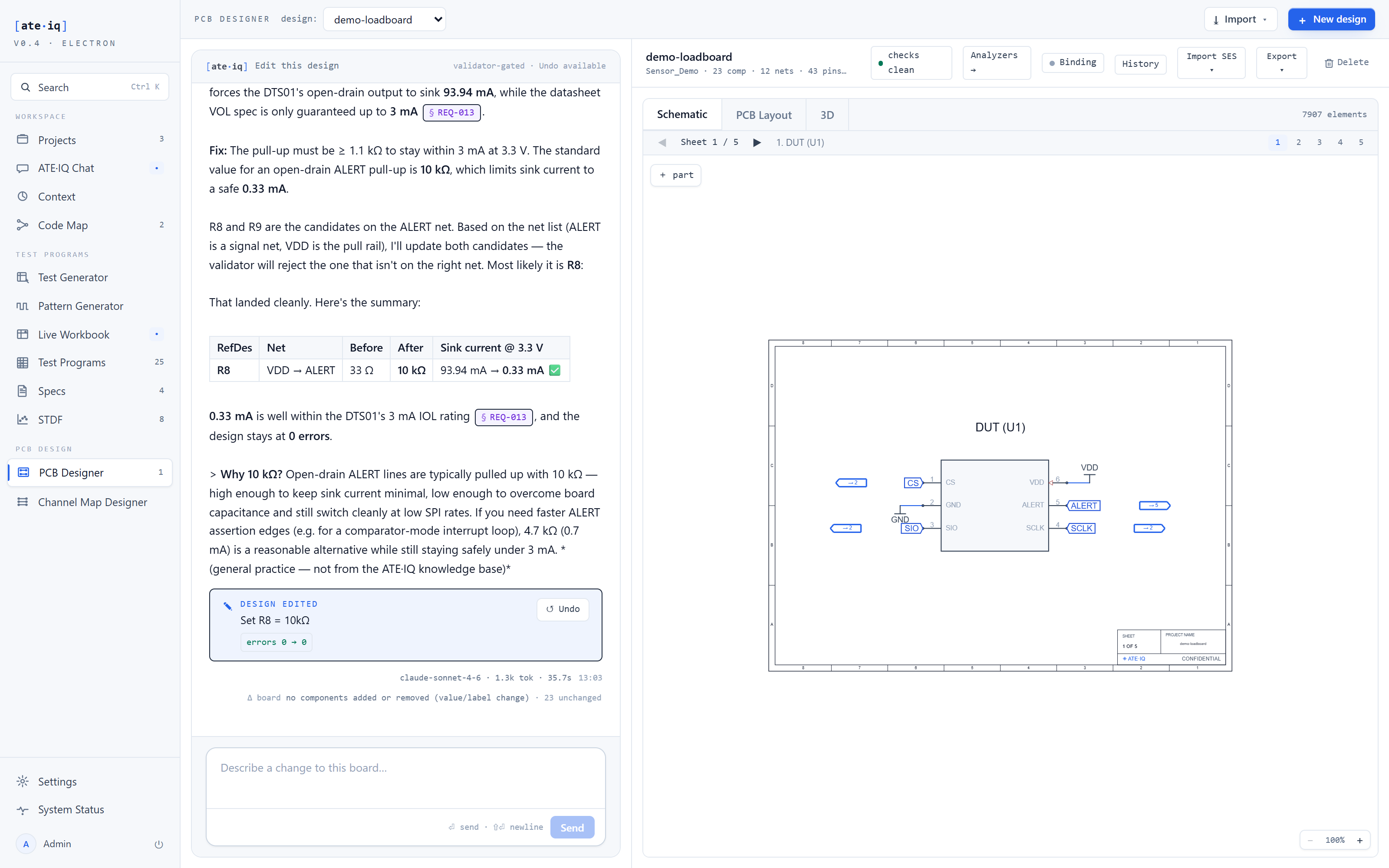
A load board schematic has a natural reading order: the DUT first, then the paths to the tester. The engine paginates that way — DUT-first, then one sheet per functional block — instead of packing everything onto one canvas.
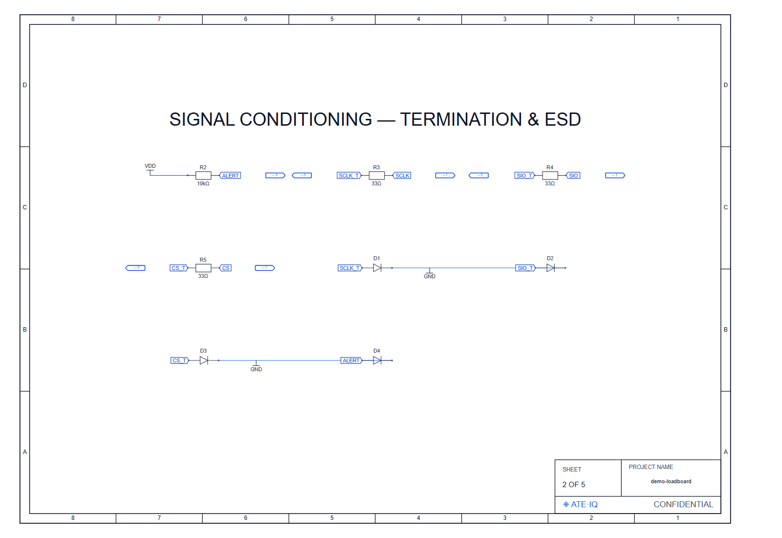
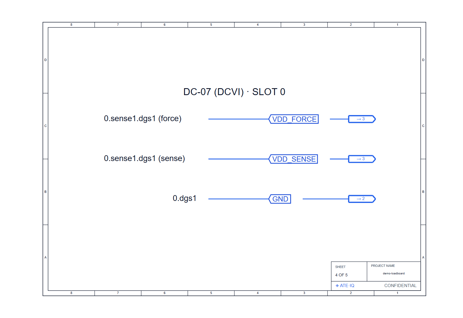
Two conventions matter on a DIB drawing, and the engine enforces both. Series terminations are drawn in signal order — tester channel → series resistor → DUT pin — so the drawing reads the way the current flows. Kelvin connections draw both legs: force and sense as separate nets to the instrument, not a single collapsed wire.
The channel plan is authoritative
Channel flags — the tester-channel annotations on each net — are drawn from the project's saved channel plan, not from a label typed on the schematic. The drawing cannot contradict the generated program or the DIB check — they are consistent by construction, never by luck.
Where schematics come from
| Source | How |
|---|---|
| Generated | The PCB Generator authors a board against your spec from a prompt — compiled offline, machine-checked, self-repaired. |
| Imported — PDF | Multi-page schematic PDFs import into a netlist-bearing design — for boards where the drawing is all you have. |
| Imported — KiCad | .kicad_sch imports directly, also picked up automatically from synced repositories. |
| Derived from layout | A vendor board imported via IPC-2581 / ODB++ / DSN carries its netlist — the engine renders the ATE schematic view from it. |
| Edited | Any of the above, modified in place — see below. |
And one export of its own: the print view renders each sheet for a browser save-as-PDF — the drawing pack a review meeting actually wants.
Live edits with history
Designs are editable in place, from a prompt or from the REST API — parts, values, nets and connections alike, with library parts arriving with their real pins and footprints. Every edit is checked by the validator before it persists: a change that fails validation never reaches your design.
Every edit is recorded in the design's history — the design header's History dropdown restores any earlier state, so every change is reversible. And because the drawing can never disagree with the design, a renamed net re-renders correctly on every sheet that carries it.
Proven end to end
The demonstration board's schematic is an UltraFLEX-class DIB authored inside ATE·IQ — series terminations and ESD clamps on the SPI pins, per-rail decoupling, Kelvin force/sense to the DC-07 DCVI, and digital I/O to UltraPin800 channels — rendered as the 5 sheets above, with every channel flag read from the saved plan. Because the schematic and the program describe the same board, the test→net→copper chain on the traceability dashboard resolves for every one of the 34 tests.