Layout
PCB Layout
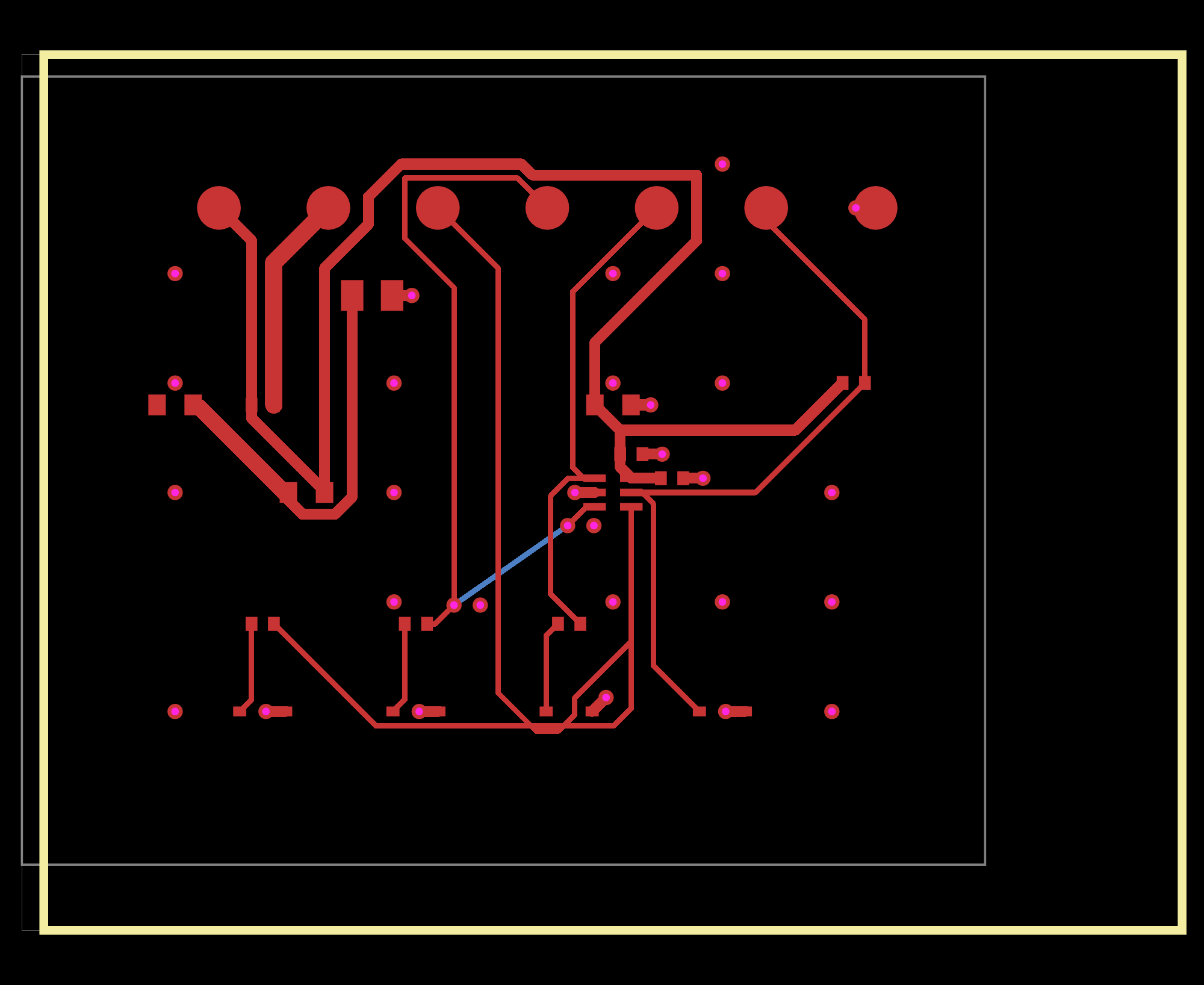
The layout is the physical board — pads, routed traces, pours, drills, layers. Your copper usually already exists in a CAD flow, so ATE·IQ's position is deliberate: import it verbatim, check it, bind it to the schematic, trace it, and export what the fab needs. No relayout is ever applied to a board someone already routed.
Layout and schematic are different things
The schematic is the logical design ATE·IQ authors and edits. The layout — this page — is the physical realisation, and its source of truth is usually your PCB vendor or CAD tool. ATE·IQ makes that copper a first-class, queryable, checkable artefact instead of a zip in a shared drive.
Every design records its provenance — which importer brought it in, or whether it was generated or hand-authored — set automatically on the way in, never by hand.
Both concerns persist in the same stored model (circuit-json), so when an analyzer reports a finding you know whether the geometry it measured came from a vendor layout or a generated draft — and the schematic and layout views can never disagree about which nets exist.
Vendor imports
A load board usually already exists somewhere — at a PCB vendor, in a legacy Allegro archive, or as a PDF nobody has the source for. The importers bring these in cold, with real copper geometry, and have been validated on real vendor boards.
| Format | Extension | Notes |
|---|---|---|
| IPC-2581 | .xml / .cvg | Full board description — components, nets, layers, copper. |
| ODB++ | .tgz | Matrix, EDA data and per-layer features to circuit-json with real copper. Validated on a 692-component rigid-flex board. |
| Specctra DSN | .dsn | KiCad, Allegro and EAGLE dialects. Pads, traces, pours, drills. |
| KiCad | .kicad_pcb | Direct board import, also picked up automatically from synced repositories. |
| Specctra SES | .ses | Round-trip: export a DSN, route it in an external tool, import the session file back onto the same design. |
Imports run from the Import menu on the design library, or automatically when a synced repository contains DSN, IPC-2581, ODB++ or KiCad files.
Copper that gets checked
Imported copper is measured, not assumed. The geometric DRC measures trace width per net class, copper-to-copper clearance and annular rings on the real geometry, each finding citing its knowledge-base rule and the measured-versus-threshold values. On top of that sit the electrical error-class gates: a same-layer different-net crossing, a trace penetrating a foreign pad, or a floating via is an error — a board that is shorted as drawn cannot pass silently. The full analyzer set is covered in Board Intelligence.
Bound to the schematic, traced to the requirement
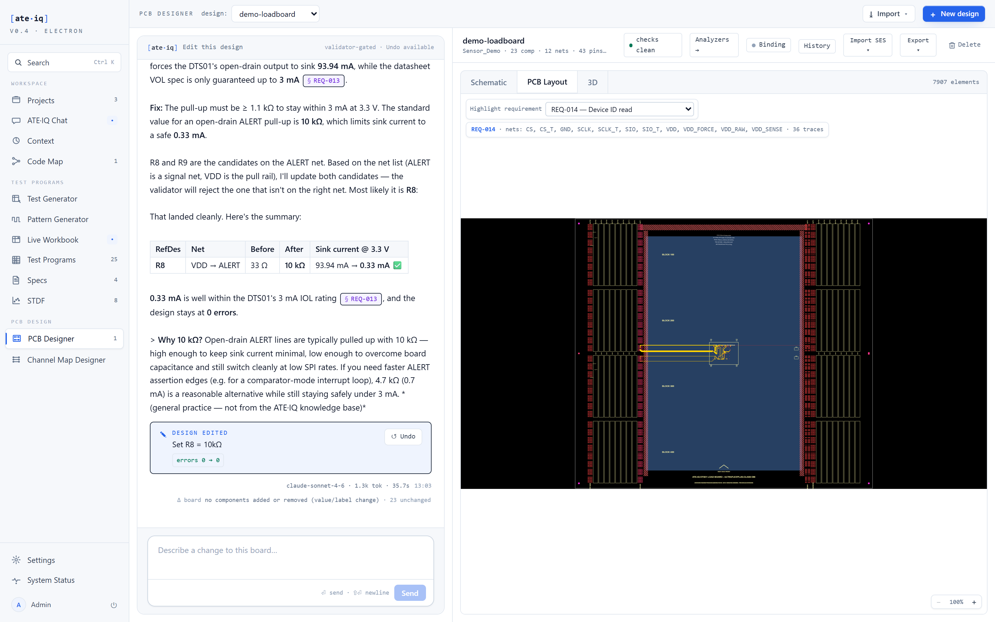
The layout binding reconciles the schematic with the routed copper mechanically — same inputs, same answer, everywhere the binding is used. That is what makes the layout more than a picture: select a requirement in the layout view and its nets light up as an amber overlay exactly aligned with the copper — consistent by construction, never by luck. Tester-side series-termination and Kelvin nets are included and disclosed as such.
Exports and the fabrication gate
Every export reads the canonical model. The full set, per design:
| Export | Contents | Gate |
|---|---|---|
| Gerber + Excellon | Per-layer copper plus drill files. | fab readiness |
| Fab package | One zip: copper, drills, BOM, pick-and-place, and a readiness README stating what the package contains and what it does not. | fab readiness |
| Pick-and-place | Placement CSV for assembly. | fab readiness |
| BOM | Bill of materials CSV. | — |
| KiCad project | Editable schematic and board files. | — |
| Specctra DSN | Routable netlist — round-trips back via Import SES. | — |
| IPC-2581 Rev C | Connectivity-only today. | — |
| circuit-json | The stored model itself, as a .circuit.json file. | — |
| Schematic PDF | Per-sheet print view; save as PDF from the browser. | — |
The fabrication outputs sit behind a readiness gate. A schematic-only design — one with no board geometry — cannot produce Gerbers that mean anything, so ATE·IQ refuses the export with the reason stated rather than emitting empty files, and the export menu warns before you click. A file you can download is a file a fab could use.
Working a board through
Import the vendor archive — IPC-2581, ODB++, DSN, KiCad or a routed SES session — and the geometry lands verbatim with its provenance recorded. The geometric DRC measures the real copper, and the electrical gates catch shorts, pad encroachment and floating vias as errors, each finding citing its rule and measured values. The layout binding puts the requirement highlight on physical copper, and the exports — Gerbers, the one-zip fab package, BOM and pick-and-place, gated on real board geometry, plus editable KiCad, DSN and IPC-2581 — feed the tools downstream.
Proven end to end
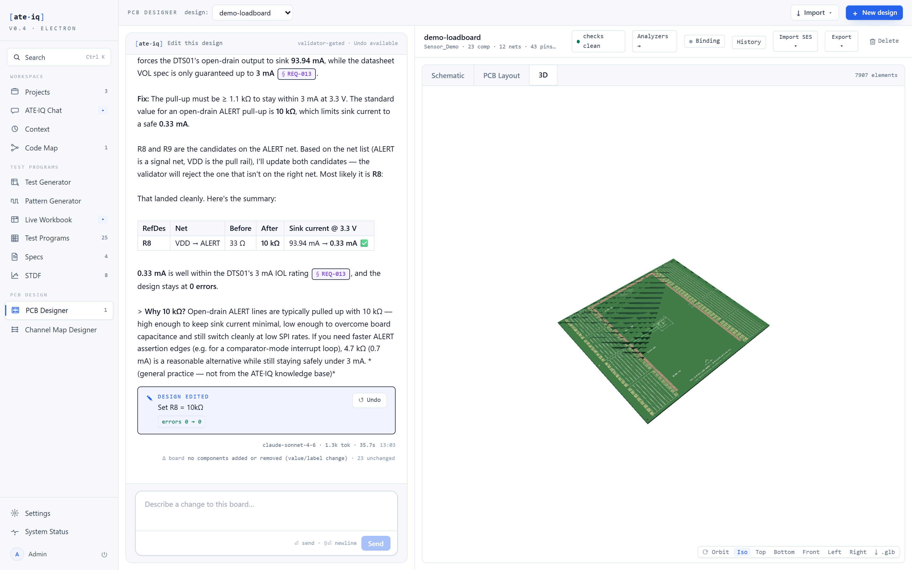
The demonstration board carries routed two-layer copper: 0.25 mm signal traces with 45° mitered bends, a 1.524 mm force run necking down at the Kelvin tap, ground pour with stitch vias, and slot contact runs to the tester edge. The electrical DRC passes with zero errors and zero warnings, and because the copper and the test program reconcile mechanically — same inputs, same answer — the requirement highlight resolves for all 34 tests.